
PHOTO ACTIVE COMPOUND
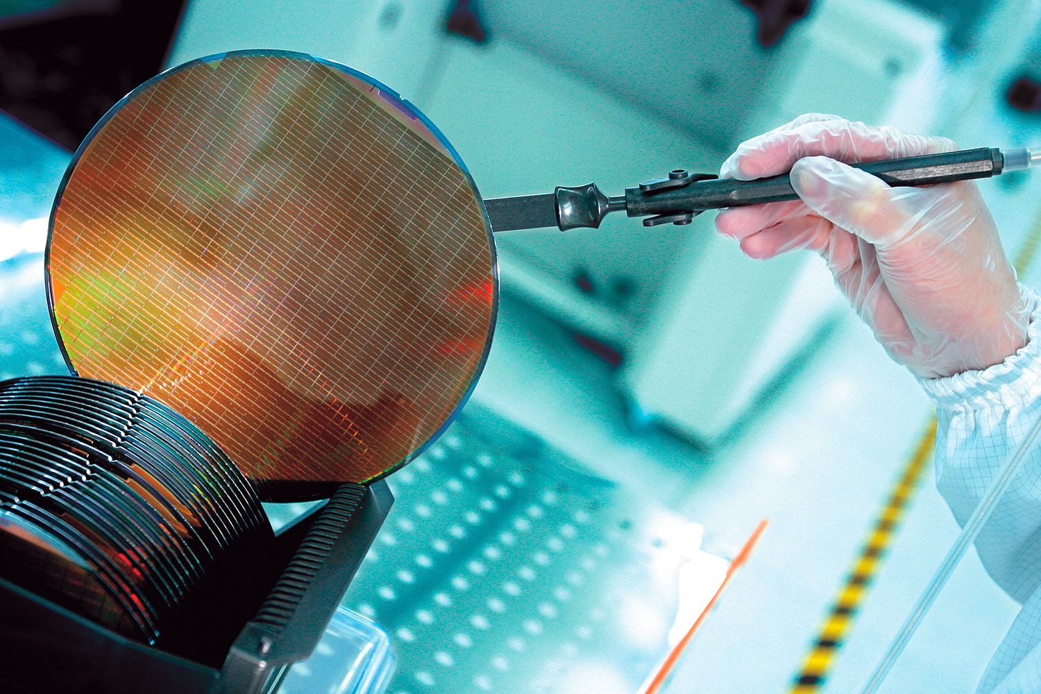
Photolithography is used to manufacture semiconductor devices and displays by transferring the image of the designed circuit onto the device. The photoresist material is applied to the substrate of the LCD, OLED, semiconductor, etc. to form a photosensitive film. Areas of the film that are exposed to light react differently allowing a pattern to develop. The key chemical in this process is the Photo Active Compound (PAC).
Daito-KISCO (DKC) was jointly established by KISCO and Japan’s DAITO CHEMIX Corporation in 2005 to manufacture and sell the core raw materials for photoresists used in display and semiconductor manufacturing processes. DKC produces and supplies photosensitive materials for displays such as LCD/OLED and high-resolution semiconductors to customers around the world. DKC is one of the three largest PAC makers in the world and is continuing to develop new PACs to meet customer requirements.
| Products include | Application include |
|---|---|
| 3-PAC, DNQ ester with Benzophenone |
Semiconductor Photoresists
|
| 4-PAC, DNQ ester with Benzophenone | Photoresists for TFTs (LCD, OLED, etc.) |
| i-Line PAC, DNQ ester with Novolac | Photoresists for Organic Insulators |
| Photoresists for LEDs | |
 |
|---|